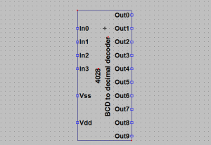
This is an article on how to simulate 4028 in LTSpice. If you need a custom IC that you know how to simulate, This method might be of interest. The principle is to create a schematics with the same name as a symbol. These files must be located in the same folder.
I made it as an sub-circuit by first creating an equivalent circuit.
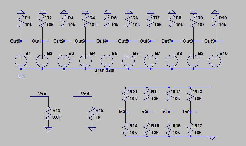
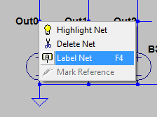
Then I labeled the nets used by the chip
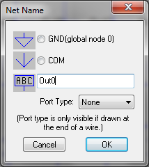
The voltage sources are actually arbitrary behavioral voltage sources to simulate the output of the 4028 chip.
B1 : V=(!(V(In3)) & !(V(In2)) & !(V(In1)) & !(V(In0)))*V(Vdd)

(logical AND of all inverse In signals times Vdd)

B2 : V=(!(V(In3)) & !(V(In2)) & !(V(In1)) & (V(In0)))*V(Vdd)

B3 : V=(!(V(In3)) & !(V(In2)) & (V(In1)) & !(V(In0)))*V(Vdd)

B4 : V=(!(V(In3)) & !(V(In2)) & (V(In1)) & (V(In0)))*V(Vdd)

...

B10 : V=((V(In3)) & !(V(In2)) & !(V(In1)) & (V(In0)))*V(Vdd)

(logical AND of all In signals times Vdd)
Then save this file as 4028.asc
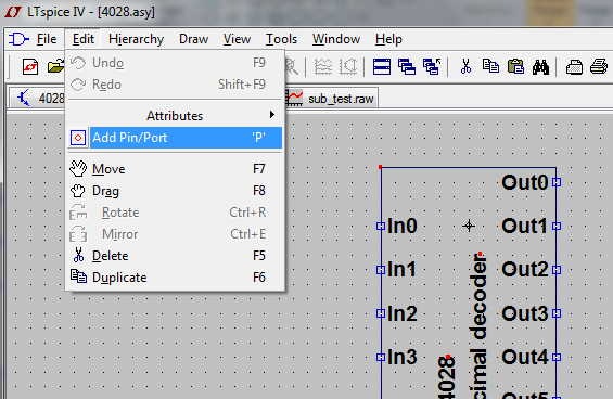
Then you have to create a symbol
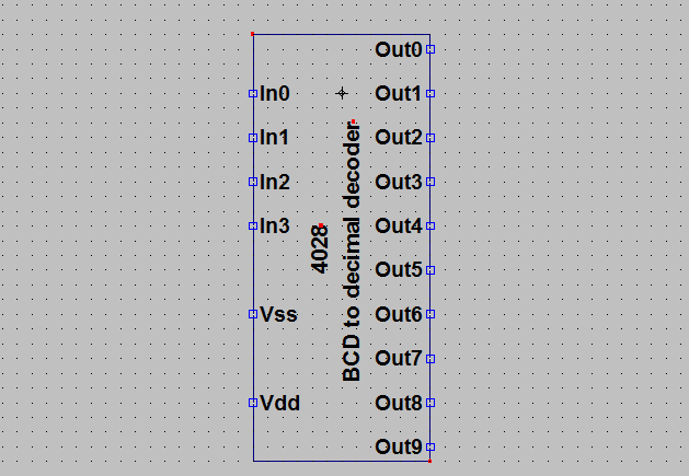
Add the same Labels you used in the .asc-file. Netlist Order should be the pin number on the chip. If you use for example number 16, all pins from 1-15 must also be defined.

Save the files as 4028.asy in the same folder as the .asc-file.
I made an extra folder in the “sym”-folder of LTSpice to have my chip.

Then I made a test circuit with two cascading 4028’s
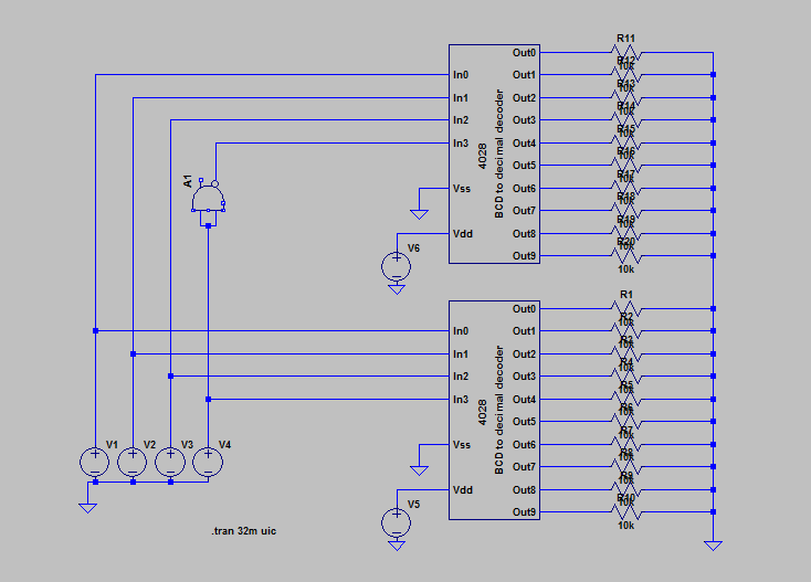
That’s it. Then there is only about 200 chips to go…
I attach the files to save you some work if you’re interested in checking it out.
http://www.lamja.com/blogfiles/4028.asc
http://www.lamja.com/blogfiles/4028.asy
http://www.lamja.com/blogfiles/4028_test.asc

