Sometimes you’ll need some given digital outputs for some given inputs in your project. At least I do. There are several ways to do this, but I will use the Karnaugh mapping method.
First let’s be familiar with some Boolean expression. If we have A and B as input of an AND gate, and the output will be C. Then the expression will be:
C = A·B
If the gate was a OR gate it will be:
C = A+B
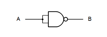
For an inverted signal I will put an underline (It should really be an overline, but since it’s easier to use underline, I will use that from now.) For an invert buffer it will be:
B = A
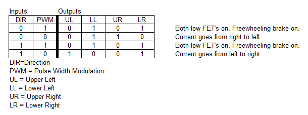
Let’s take an example. A H-bridge will take two inputs, direction and PWM-signal. We will have to convert those signals to the correct combination for the four MOSFET’s in the bridge. By doing this, we also assure that there will be no shoot-through, shorting the power supply by opening high side and low side at the same time.
Next step will be to map the two inputs as a Karnaugh map.
As you see we have to find groups or blocks of 1’s to get the simplest solution. If the block goes over a whole row or column, the result is the signal that do not change. If it say 0, it should be the NOT variant of that signal.
If the result is just a digit, its the AND of both signals.
If you have to use two blocks to get all, put a + sign in between.
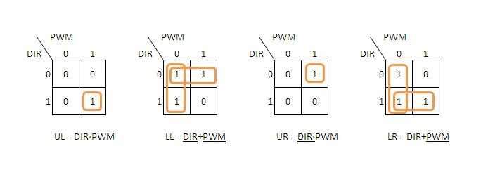
In the LL table the upper block is DIR because it’s on the row DIR=0.
In the LR table the lower block is DIR because it’s on the row DIR=1, and the left block is PWM because is located on the column where PWM=0.
You can read more about this on Google Books:
http://books.google.com/books?id=xqLl9_YwYn4C&lpg=PP1&pg=PP1#v=onepage&q&f=false
UL = DIR·PWM
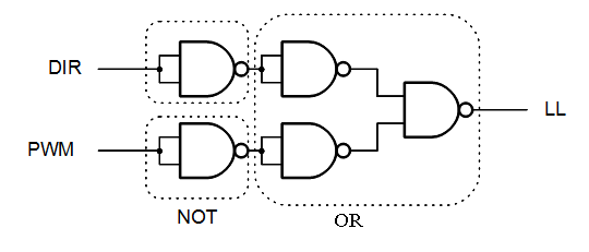
LL = DIR+PWM
UR = DIR·PWM
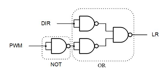
LR = DIR+PWM
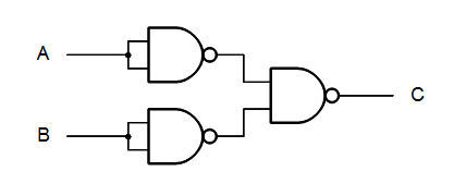
We have some NAND-equivalent for NOT, AND and OR gates like this:
Two NOT’s in serial will cancel each other out. It will then look like this:

Removing the two NOT’s in serial it will look like this:

By using De Morgan’s Theorem on UL we get:
UL = DIR·PWM = (DIR+PWM) = LL (NOT(NOT(DIR)+NOT(PWM))
This is actually easy to see, from the two truth-tables UL and LL. LL is the inverse of UL.
The same is true for UR and LR
UR = DIR·PWM = (DIR+PWM) = LR
Then we can put it all together to this:
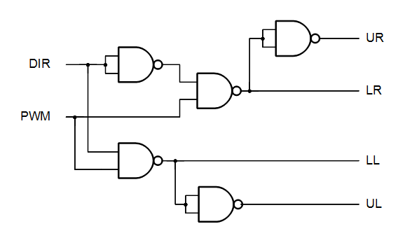
The actual H-bridge that I am designing, upper left (UL) and upper right (UR) uses an extra MOSFET for driving the H’bridge’s FET’s. This will cause an extra inverse operation on the signal from the logic to the FET’s. We then don’t need the signals UL and UR, but instead we’ll need UL and UR, wich is actual LL and LR
The total simple schematic will then be:

Complete H-bridge design will follow in some future blog entry.
Feel free to leave a comment below.



go